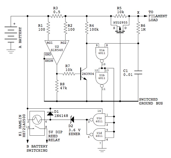
On another one of my webpages, I describe a battery powered boost converter that can be used as the B supply for antique battery powered tube radios. The use of a boost converter allows the battery supply voltage to be 6 to 9 volts rather than the inconvenient 90 volts of the original B batteries. When the radio is switched off, the user must remember to shut off the boost converter or else it will continue to use battery power, and eventually drain the battery. To make things more automatic, it's possible to monitor the filament voltage inside the radio, and when it is detected, the boost converter can be switched on by means of a small relay. However, that involves some invasive internal wiring of the receiver. It would be better to keep the battery pack completely self contained with no additional wiring of the receiver. One way to accomplish this is to monitor the current of the filament battery, and when current flow is detected, the boost converter is switched on. This allows the battery pack to be a drop in replacement for the original. Such a circuit is shown in the picture below.

The design of the filament current sensing circuit poses one significant challenge. When the radio is off, then this circuit must not draw any power. Otherwise, we are back to the problem of the battery being drained when not in operation. The circuit to be described here draws only about 40 nA (nanoamperes) when the radio is off. This is roughly equivalent to the current that would leak from the battery due to imperfect insulation in the battery itself. Consequently, the battery will last for its normal shelf life when the radio is off.
The circuit makes use of a very low power current sense amplifier (Silicon Labs Si8540) which draws 90 µA in normal operation, and only 9 µA in shutdown mode. However, the off state current draw of the complete circuit is lowered by another couple of orders of magnitude by the use of a CMOS logic IC and a two stage operating mode. The CD4011 quad two input NAND gate IC draws only about 40 nA when it's not switching (i.e., in steady state). This characteristic is used to great advantage.
Operation
The circuit will operate with a filament battery ranging in voltage from 5 to 15 volts. This limit is set by the minimum and maximum operating voltages of U1 (3 to 15V) and U2 (5 to 36V).
Referring to the schematic below, the voltage on the line labeled "Switched Ground Bus" is controlled by the output of NAND gate U1b. When the radio is not drawing any filament current, the output of this NAND gate is equal to the positive battery voltage. This puts every point in the circuit, except one, at the positive supply voltage. Since everything is at the same voltage, there is no potential difference, and therefore no current flow. The only exception is the quiescent current of U1 which is 40 nA. Note that pin 7 of U1 is the only part of the circuit that is connected, via ground, back to the battery negative terminal.

With the radio drawing no filament current, both inputs to U1a are logic 1. Its output is logic 0, and U1b connected as an inverter, then has an output of logic 1 as previously stated.
When the filament load is applied, it is a much lower resistance than R5, and so the voltage at point X (upper right of the schematic) drops to near zero volts. The voltage at pin 8 of U1 starts to drop, delayed by the time constant of the R6-C1 network. When it reaches logic 0 voltage, the output of U1a changes state to logic 1, and consequently the output of following gate U1b goes to logic 0, or ground potential. This pulls the switched ground bus down to true ground potential, thus activating the rest of the circuit. Since one side of C1 is connected to the switched ground, this provides a positive feedback effect, pulling pin 8 of U1a down hard, and preventing the possibility of it drifting back up to an indeterminate logic state before the rest of the circuit becomes operational.
With the switched bus at ground level, U2 is now operational and begins sensing battery current flow. The gate of the P-channel MOSFET Q2 is now grounded, switching the transistor on fully, bypassing the 10k current limiting resistor R5 and thus applying full voltage to the radio’s filament load. The filament current is now sufficient to cause the output of current sensor U2 to rise, switching on transistor Q1 which pulls down pin 9 of U1a to logic 0. At the same time, pin 8 of U1a is starting to rise, but as long as one of the U1a inputs is at logic 0, the output of U1a will remain high, and the switched bus will remain at ground potential. The circuit has now fully changed over from its ultra low power sensing mode, to a higher current operating mode, with U2 now providing the load current sensing.
The output of U1a also goes to the inputs of gates U1c and U1d whose outputs are connected in parallel and act as a buffer stage. Their outputs are now at logic 0 state, and energize the coil of relay K1, which switches on the B supply boost converter. All power is now available to the radio receiver.
When the radio is switched off, the filament current drops to zero, and this is sensed by U2. Its output drops, switching off transistor Q1, which causes pin 9 of U1a to go to logic level 1. Pin 8 is already at logic 1, and so U1a output goes low. This causes the output of U1b to go high, bringing the switched ground bus back up to the positive supply voltage. Relay K1 drops out, shutting off the B supply boost converter. The circuit is now back in its ultra low power state.
The circuit, as presented, is sensitive enough to sense current flow of less than 30 mA. This is plenty of safety margin, since the lowest filament current in common production vacuum tubes is 60 mA. The tubes in the Zenith Transoceanic, for example, are all 60 mA filaments. The six tubes in this receiver have 1.5 volt 60 mA filaments which are connected in series for a net 9 volt 60 mA load.
Zener diode D2 may or may not be required in the circuit, depending on the the voltage of the A battery. For a 6 volt battery, D2 may be replaced with a jumper. For a 9 volt battery, the 3.6 volt zener should be used, because the relay coil is rated at 5 volts. The amount of current that can be delivered to the relay coil is also limited by the maximum current capability of the CMOS gate output. So, it’s unlikely for any damage to occur to the relay, in any case. But this puts less stress on the CMOS gate output. For higher filament battery voltages, the zener diode voltage rating should be about five or six volts less than the battery voltage.
The off-state current consumption was previously stated as being about 40 nA. When current is being drawn and the circuit changes mode, the current consumption will increase. U1 will continue to draw 40 nA. U2, according to its data sheet, will draw 90 µA. U2 output will be about 3 volts. Transistor Q1 will have a base current of about (3 – 0.7)/47,000 = 49µA, and collector current of 5/100,000 = 50µA. So far, this is a net current of 90+49+50=189µA. However the largest current draw will be the coil of relay K1. It has a resistance of 500 ohms. At 5 volts, it will draw 10 mA, making the other loads insignificant.
Alert readers may wonder: why did I choose to use a relay to switch the B supply, rather than using another power MOSFET? I admit, a relay certainly would not have been my normal first choice. However, I wasn't able to find a power MOSFET having a low enough off-state leakage current, while still meeting the other circuit requirements. Having reduced the A battery off-state current to 40 nA, I wasn't willing to settle for any less on the B battery side of the circuit. For that reason, I ultimately chose to use the small DIP reed relay. Nothing is ever final, of course. If I manage to find a suitable power MOSFET with a leakage current in the low nanoamp range, then it will become the device of choice. But, until that happens, the relay will do the job.
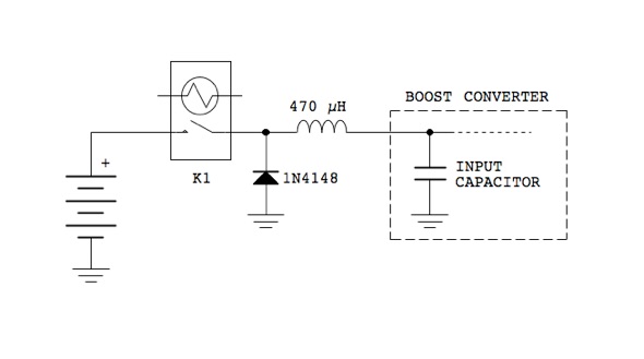
A word of warning however: for the relay shown in the schematic, the maximum switching current for its contacts is only 500 mA. Assuming a boost converter that up-converts from 9 to 90 volts to deliver 25 mA to the radio (typical for a Zenith Transoceanic model receiver), and assuming a modest efficiency of 70%, this equates to a current draw on the low voltage side of 360 mA, which is within the relay's rating. However, one still needs to be cautious of switching a highly capacitive load, which is certainly the case for a the boost converter. For this reason it is wise to include a small current inrush limiting inductance in series with the relay contacts, and then a protection diode to prevent high reverse EMF when the relay opens. This is shown in the following diagram.

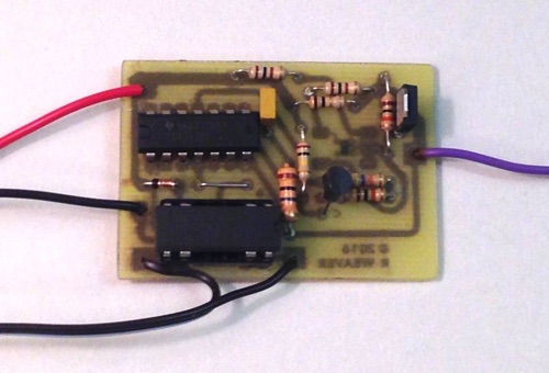
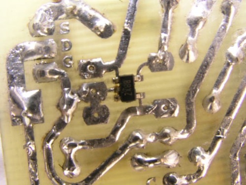
The circuit was built on a small printed circuit board. The completed unit is shown in the photo at the top of this page. All components, except for the current sense amplifier U2, are traditional through-hole components. The Si8540 current sense amplifier is a very tiny SOT-23 surface mount component, measuring 2 mm by 3 mm. I had some misgivings about using this device, because of the difficulty in mounting it, but it worked so fabulously well in the breadboard prototype circuit that I decided to go with it. I’m now at a stage where I’m willing to allow one surface mount component per project. If nothing else, it does force me to practice using these things. However, the circuit board was designed in such a way that it allows several different mounting options for this chip. It may be soldered directly to the foil side of the board if the builder is sufficiently confident and has steady hands. It may also be mounted to a breakout board, and then the breakout board soldered to a larger set of solder pads on the main board. The use of a breakout board is also handy for prototyping the circuit on a breadboard. A third mounting method is to use ‘dead bug’ style mounting; i.e., mount it upside down, legs in the air, on the component side of the board with a drop of superglue, and then tack solder some fine wire leads from the device pins to the circuit board solder pads. However, I was feeling brave, and soldered the device directly to the foil side of the board. Really, it is good to gain some experience with these devices, as eventually there will be no other choice but to use them. Below is a closeup photo showing the mounting of U2.

Notice that the Si8540 is about the same size as a normal through-hole solder pad. The set of larger solder pads surrounding the Si8540 are for the use of a breakout board mounting option. My method for mounting these tiny surface mount chips is explained on this page.
The circuit board was made using the laser printer toner transfer method. I won’t go into the details on that, because there is already plenty of information available on the Internet.
The printed circuit layout pattern and component mounting can be downloaded here. The foil pattern is mirror image, suitable for toner transfer fabrication. The foil pattern file also includes some breakout board foil patterns for separate mounting of U2, should that be desired.
The circuit board design does not include the B supply inrush current limiting components described above, as different boost converters may have different inrush characteristics. So the builder must incorporate them separately.