
Updated 2020-02-11, to use a faster
microcontroller with additional software features.
Updated
2022-11-16, to allow the use of keyboards with different key wiring
arrangements.
The Analog Devices AD9850 and AD9851 are inexpensive and popular DDS (Direct Digital Synthesis) signal generator chips which produce a decent quality sine wave output over a continuous frequency range from less than 1 Hz to around 40-70 MHz with a resolution finer than 1 Hz. Such chips have many practical uses. However, unlike many chips which can be controlled by connecting a few simple external components such as pushbuttons or potentiometers, these DDS chips use a digital interface (both parallel and serial are available). They require a microcontroller to send the appropriate control data to set up the operating parameters. This may put them out of reach of hobbyists who haven’t the means to deal with microcontrollers. I’ve worked with microcontrollers over the years, and I decided to program a PIC microcontroller to provide a simple user interface to these DDS chips. The first part of this article discusses the circuit hardware, and construction. All of the design files required for building the various circuit boards can be downloaded from the link given at the bottom of this page. In Part 2, of the article, the software is discussed.
Let me digress for a moment, to mention that the AD9850 and AD9851 are not state of the art chips. They were developed in the last century—the 1990’s. If they had been developed recently, they almost certainly would be sporting a more developer friendly interface. A significant shortcoming is the inability to read data back from the chip. If you send it the necessary instructions to operate at a certain frequency, you have no way of confirming that the data got to the chip error free, other than to use external frequency measurement circuitry. Other than that, the interface is not a major problem.
Another issue—I’ve been advised that these chips have a high enough level of phase noise that they are unsuitable for use in high performance communications receivers. This is beyond my area of expertise. I recommend referring to the various amateur radio sites published by people who do have the expertise. Still, these are very useful chips with many applications for the hobbyist. They can be used to make a general purpose sine wave signal generator that will easily outperform an older shop grade RF signal generator by many orders of magnitude. They may not be perfect, but they should prove useful to many people who dabble in hobby electronics.
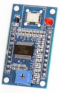
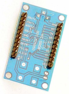
The AD9850 and AD9851 are currently available in the form of small modules which include a reference clock oscillator, output low pass filter, and a few other passive support components. Using these modules greatly simplifies the work involved in getting the DDS chip up and running. The modules are available from many sellers over the Internet, and have the generic part number: HC-SR08. Doing a search for this part number will result in many hits. Front and back pictures are shown below.


The same HC-SR08 part number is used for both the AD9850 and AD9851 versions. So, it’s important to check the product description to find out which one is being offered. The only significant difference is that the AD9850 typically comes with a 125 MHz reference frequency oscillator, and the AD9851 typically comes with a 30 MHz reference frequency oscillator. The AD9851 has an internal 6× frequency multiplier circuit which gives it an effective reference frequency of 180 MHz. The maximum usable output frequency is roughly 40% of the reference frequency which means the AD9850 is good up to about 50 MHz, and the AD9851 is good up to about 70 MHz. The waveform starts to degrade above 1/3 of the reference frequency. So, the practical upper limit depends on how much waveform degradation one is willing to accept. In any event, due to Nyquist limits, the output cannot go above one half of the reference frequency.
From examining these modules, the onboard circuitry is fairly minimal. It includes the reference frequency oscillator, an output filter that appears to be similar if not identical to the one shown in figure 29 of the AD9851 datasheet, and a potentiometer for adjusting the square wave output pulse width (not used in this project). All other signal lines from the AD9850/51 are brought out to the header pins. I point this out, just in case the HC-SR08 becomes unavailable at some future time, and one wishes to reproduce the circuit.
Data sheets for the DDS chips are available here:
Other than frequency range, the chips are nearly identical, having the same pinout. Both versions of the HC-SR08 modules have identical pinouts as well. The data format of both chips is also virtually the same, so the control algorithm in the external PIC controller is identical for both except for minor configuration differences. It is necessary only to change some parameter data to account for differences between the reference frequencies (and reference frequency multiplier).
As mentioned above, the AD9850/51 has both a parallel and serial interface. In order to save I/O pins and reduce wiring, I chose to use the serial interface. With the serial interface, only three signal lines are required: Data, Clock and Latch. There is also a Reset line, which I included in the first version of my interface, but I eventually dropped it, because I found that it didn’t appear to be necessary, and I needed to free up an I/O pin on the PIC as I added other features. Later on, on rare occasions I did find that the chip was not properly reset upon power up. To address this, I added a resistor/capacitor/diode network to the DDS circuit board that holds the DDS chip in reset mode for a short time during power up. In addition, the software in the controller can initiate a reset at any time by holding the DDS clock line high for at least 1 millisecond.
When I first decided to build this interface, I wanted to make it as general as possible. I wasn’t tailoring it to any specific application that might need only a small frequency range or certain fixed frequency increments. Yet, I did want the ability to set, with a resolution of 1 Hz, any frequency that the DDS chip is capable of producing. Rotary encoders are popular input devices for DDS interfaces. It’s hard to argue against the convenience of twisting a knob to adjust frequency. However, after much consideration, I decided that it wasn’t very convenient to use an encoder to set an 8 digit frequency value. Either it would require several encoders: one for each digit, or else some extra pushbuttons to pick which digit the encoder is setting. Going back and forth between pushbutton and encoder makes for cumbersome operation. And so I finally decided to use a numeric keyboard. I don’t recommend using cheap membrane type keypads though. Good quality numeric keyboards with full travel keys make a big difference in ease of use. Good keyboards are not hard to find. They can be salvaged from old desktop calculators. (In a later version of the project, I did include the option for encoder input. This is described in Part 2.)
For frequency display, I chose the popular type 1602 2-line × 16-character LCD display that uses the industry standard HD44780 interface. It doesn’t look very fancy compared to the newer multi-colour graphic displays, but it’s practical and cheap.
For the microcontroller, I chose a Microchip PIC16F630. I had several of them on hand, which influenced my decision. It’s a basic 14 pin controller, which appeared to be more than adequate, before feature creep began to set in. I’ve now updated to a PIC16F1703 which is 60% faster, and has twice as much program and data memory. The new chip is a drop in replacement, needing no circuit modifications. In fact, since it uses its own internal clock, the external ceramic resonator and associated capacitors can be omitted. The enhanced features of the newer chip will be discussed below.
In the original prototype I used the internal 4 MHz clock of the PIC16F630, which was fine for a fixed frequency output. However, I later added a frequency sweep function to the circuit, and the 4 MHz clock wasn’t able to give a fast enough sweep rate to avoid excessive flicker on the oscilloscope. So, I added an external 20 MHz ceramic resonator which gave a good boost to processor speed but required the sacrifice of two I/O pins, and the consequent necessity of doubling up of some pin functions. Ultimately, this resulted in a more efficient design. However, the small memory size became the next limitation. With the added sweep functions, it was maxed out. The newer PIC allows for more features.
The only drawback to the PIC16F1703 is that it cannot be programmed with the older PICkit2 programmer. It requires the newer PICkit3 programmer. This had been a consideration at the time, because PICkit2 compatible programmers were available from Internet vendors much cheaper than the PICkit3. However, PICkit3 compatible programmers have now become inexpensive as well.
For a power supply, I kept things as simple as possible by using an external USB type 5 volt DC supply, of the type used as cell phone chargers.
The total parts cost is around $25. That is excluding the cost of the numeric keyboard (which one should be able to scrounge up from a junk desktop calculator or computer keyboard).
As mentioned above, frequency entry is by means of a numeric keyboard, wired as a 3 row, 4 column matrix. This allows for 12 keys, digits 0-9, a Clear key “C” and a Line Select key “+/−”. In addition to the keyboard, there are two pushbuttons, “+Incr” and “–Incr”, and a 4 position rotary switch for mode selection. The operational modes are as follows:
In Frequency Direct Entry mode, frequency is entered in Hz, up to 8 digits, directly from the keyboard. As shown in the picture at the top of this page, the top line of the display shows F (short for Fo, the centre frequency) on the top line and + on the bottom line (short for F+, the frequency increment, or sweep range). A right arrow indicates the active line for keyboard entry. The frequency entered in the top line is the primary or centre frequency. The output of the DDS signal generator updates instantly as frequency Fo is entered. The second line is for entering a secondary frequency which will be described below. The +/− key toggles between the upper and lower line of the display for selecting numeric entry of either Fo or F+.
In Frequency Up/Down Increment mode, a primary frequency Fo must first be entered in direct entry mode, as well as an increment frequency F+. After setting these in direct entry mode, the output frequency will increment up or down by the increment amount when the +Incr and –Incr buttons are pressed. For example, if 1000,000 is entered for Fo and 2500 is entered for F+, then the frequency will start at 1 MHz and each press of the +Incr or –Incr button will increment or decrement the output frequency by 2.5 kHz. The primary purpose of this mode is allow the user to step up and down by the fixed channel spacing of radio stations (when using as a local oscillator or a frequency spotter), or by other fixed amounts when doing frequency response measurements. For example the primary frequency can be set to 540 kHz, and the step amount can be set to 9 or 10 kHz (depending on the local broadcast band channel spacing). Then pressing the +Incr and –Incr buttons will step up and down in exact channel increments.
In Sweep mode the circuit sweeps over the range Fo–F+ to Fo+F+ (centred on Fo), in either 128 or 255 steps, depending on which of the two sweep modes is selected. As before, Fo and F+ must first be entered in direct entry mode, and then the selector switch moved to one of the sweep positions. In Sweep-128 mode, the sweep repeats about 60 sweeps/second for the 16F630. So, scope traces in this mode are completely flicker free. In Sweep-255 mode, the sweep repeats about 30 sweeps/second for the 16F630, and some minor flicker is visible on the scope trace. For the 16F1703, the sweep rates are 96 and 48 sweeps/second for the respective modes, and are flicker free for both.
To facilitate displaying sweep traces on a scope, the circuit also provides a linear ramp output, proportional to frequency, which can be connected to the horizontal input of the scope in X-Y mode. Below is a trace of a 455 kHz ceramic filter response curve using this feature.
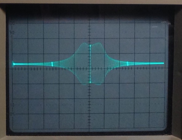
The above example is using 128 step mode. The individual frequency steps are visible as distinct vertical lines. In 255 step mode, the individual frequency steps merge together giving a smoother frequency response trace as shown below, but there is some flicker because the scan rate is now half that of the 128 step mode.
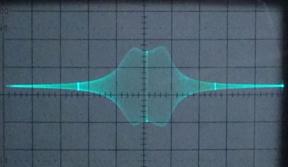
In both photos, you can see intensified markers positioned at the centre frequency, 25% frequency, and 75% frequency. This is accomplished entirely in software by having the sweep pause briefly at each of these frequencies causing the trace to intensify at these locations.
One subtle detail is that in 128 step mode, there are 128 frequency steps or increments. Counting the starting frequency plus the 128 increments, there are actually 129 discrete frequencies in the sweep, with the 64th being the user-entered centre frequency. Thus, there is the same number of discrete frequencies on either side of centre. In 255 step mode, there are 256 discrete frequencies in the sweep: an even number. This is the maximum count that can be accommodated in the single byte counters, and therefore the maximum number of discrete analog output values in the sweep output ramp signal. What this means is that in 255 step mode, the user-entered centre frequency will occur at step 128 which will not be the exact centre of the sweep. Ideally, there would be one final increment (256) at the upper end of the sweep to display a 257th frequency for things to be perfectly symmetrical on either side of the centre frequency. In any case the centre frequency is clearly identified by the marker. So, this has no effect on operation.
A primary goal was to keep the component count as low as possible, and just provide the bare necessities to control the DDS chip. However, I did give in to temptation, and provided circuitry for the sweep ramp output as previously mentioned. This added about a dollar to the cost, and minor additions to the circuit (and that part of the circuit can simply be omitted if it’s not needed). The schematic diagram is shown below.

The circuit is simple enough that I assembled the original prototype on a standard solderless breadboard as shown here.

To control the DDS module, only three signal lines are required, W_CLK, DATA, and FQ_UD (latch). These are connected to pins 10, 11 and 12 of the PIC.
Some HC-SR08 modules are supplied with 3.3 volt oscillators instead of 5 volt oscillators. This creates a minor problem when operating from a 5 volt supply. The oscillators can overheat and eventually fail. The PIC can also operate from 3.3 volts, but the LCD display must operate on 5 volts. The simple solution is to operate the circuit on 5 volts, and provide current limiting resistors between the PIC outputs and the DDS inputs. In addition, the supply voltage to the DDS is dropped to a safe level using two 1N4007 diodes in series. The circuit as shown includes these provisions. If the module is supplied with a 5 volt oscillator, then the dropping diodes can be omitted (replaced with jumpers), but it’s a good idea to keep the resistors in the I/O lines because they have the added benefit of providing noise isolation between the DDS module and the rest of the circuit.
The numeric keyboard, the +INCR/–INCR pushbuttons and the rotary selector switch are interfaced to the PIC using a 74HC165 8-bit parallel in/serial out shift register. The mode select switch is a binary coded rotary switch. For four positions, it has two binary coded outputs:

For the binary coded rotary switch, I used one that I had on hand. While doing this writeup, I discovered that the part is now obsolete. There are other suitable BCD and HEX coded rotary switches available, but it may be just as easy to use a regular single pole, 4 position rotary switch with some diodes to code the same 2-bit output. The diode type is not critical. Suitable diodes are 1N914, 1N4148, 1N5711 or even 1N4007. The switch wiring is shown below.
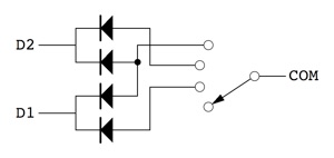
Mode 1 is the bottom position, and mode 4 is the top position.
To read any of the user inputs, the PIC toggles the 74HC165 LOAD input (pin 1) to load the current state of all eight inputs into shift register, and then toggles the clock line (pin 15) 8 times to shift the data over the serial output (pin 9) into the PIC. This will directly read the +INCR/–INCR pushbuttons and the rotary selector switch. To read the keyboard, this operation must be repeated three times, with each row of the key matrix being set high in sequence between each read.
The numeric keyboard layout is arranged in the schematic to show how each key is arranged electrically (rather than physically) in the matrix. Pressing a key, connects the row and column lines that pass under the key. The arrangement used with this circuit makes for simple conversion of a key’s numeric value to its binary value. When dealing with a salvaged calculator keyboard, the wiring may be different than shown here. Most keyboards that I’ve encountered have discrete pushbuttons for each key, with the matrix arrangement set by the pattern of the circuit board to which the keyboard is attached. It may not always be practical to desolder the keyboard from the circuit board. Instead, the traces on the board can be cut with a utility knife or Dremel tool (the older keyboards usually use single sided boards with the traces easily accessible). Then the pushbuttons may be reconnected in the required arrangement with hookup wire.
One of the new features of the 16F1703 version is the option to use any numeric keyboard having any key wiring arrangement as long as it's a 3×4 or 4×3 matrix. This is accomplished using a lookup table to translate the incoming keycode to that which is expected by the program. The custom wiring of the keyboard matrix, described in the previous paragraph, saved limited memory in the 16F630 version. However, this restricted the choice of keyboards to those having wiring access to each key. Telephone type keyboards are inexpensive and widely available from Internet vendors, but most have inaccessible key wiring. The new version of firmware, discussed in Part 2, will work with these and other keyboards without the need to make any changes to the wiring.
The sweep ramp output is generated by means of a simple 8 bit D/A convertor which uses a 74HC595 serial in/parallel out shift register, and an R-2R resistor network. The PIC sends the 8 data bits for the analog signal to the 74HC595 serial input (pin 14) toggling the clock input (pin 11). Once all bits have been loaded, the output latch is toggled to send the parallel value to the R-2R resistor network to generate the analog value. The R-2R network that I used is a Bourns 4610X-R2R-103LF, with R=10k and 2R=20k. The resistance values are not critical; the value of R can range from 1K to around 20k with negligible effect on performance. I chose the 10k network because it is a stock item at Digi-Key. As an alternative, the R-2R network can be constructed with discrete resistors. For my original prototype, I used 1% resistors mounted on a piece of veroboard as shown below.
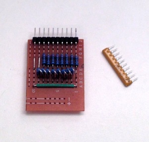
The yellow item to the right is the Bourns 4610X-R2R-103LF network. Either one will work fine, but the Bourns R-2R network is a bit more precise, making for a marginally more uniform scope display, and it’s much more convenient to use. Since I needed to place a parts order anyway, I stocked up on these networks, because they make a handy 8-bit D/A converter that doesn’t require the low pass filtering that a PWM type D/A output would require.
On the subject of resistor values, most of the resistors used in this circuit are not critical since most are used as pull-ups or pull-downs. Values can vary quite a bit without affecting performance. The pull-down resistors on the 74HC165 inputs can vary between 1k and 50k. I happened to have some 8×10k resistor networks which made for convenient construction. However, separate resistors can easily be substituted.
I designed a single sided printed circuit board for the controller circuit that is suitable for the toner transfer method of circuit board fabrication. The links to the files are at the bottom of this page. For anyone deciding to make one of these boards, I apologize that I don’t have files available in standard PCB file formats. I’ve used a generic CAD drafting program, not one designed for printed circuit work. I’m still on the low end of the learning curve of Eagle CAD. Hopefully, that will change before too long.
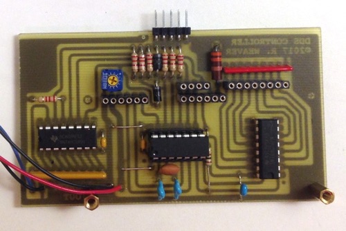
The main controller board is laid out so that the LCD display can be piggybacked directly on top. Located on the main board are mounting hole centres which should be correctly positioned for most versions of the 1602 LCD display.
The connection to the keyboard, pushbuttons and rotary switch is by means of a single row 14 pin header (directly above the LCD connector).
It was my intention that the DDS module would be mounted separately from the controller board. Because of the high frequencies generated by the DDS module, it makes sense to keep it isolated and possibly shielded from the rest of the circuit. This is no serious inconvenience because there are only two power supply lines and three signal lines connected between the controller board and the DDS module.
However, the DDS module does require a small amount of additional wiring. Two 10k resistors, a 1N5711 diode, a 0.1 µF capacitor and a few jumpers are required (see schematic above). I used a small piece of Veroboard with two 10-position female headers to mount the DDS module. The components and jumpers are mounted on this board as well. For these few connections, it didn’t seem worth the effort to make another printed circuit board at this time.
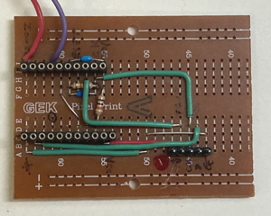
The purpose of the connections to data lines D0, D1 and D2, is to set the DDS chip to serial data mode. Upon power up, and after a hard reset, the chip defaults to parallel mode. With data lines D0, D1 and D2 hardwired this way (parallel data input = binary 011), it requires only a pulse on the W_CLK line followed by a pulse on the FQ_UD line to set the chip to serial mode.
The remaining resistor capacitor and diode comprise the reset circuit. (This was not shown on the schematics or circuit board layouts prior to the 2022-11-16 update.) When power is applied to the circuit, the PIC I/O lines are in high impedance state and with one side of the capacitor connected to +Vcc, the reset line is immediately pulled high, holding the DDS in reset. Once the PIC has initialized, it pulls the clock line low, and the capacitor discharges through the diode, pulling the reset line low. This causes the DDS to start normal operation. When the PIC sends data to the DDS, the positive clock pulses are too narrow to affect the reset line due to the long RC time constant. However, the PIC can reset the DDS whenever necessary, simply by raising the clock line to logic 1, and holding it there for a few milliseconds.
As mentioned above, my intention was to keep the circuit as simple as possible while still allowing for future enhancements. Also, I didn’t want to add any additional circuitry that would require supply voltages other than the single +5 volts.
On the controller board I didn’t bother to add a buffer for the D/A sweep ramp output. The input impedance of an oscilloscope is high enough that buffering is unnecessary. However, if there is a need to drive a lower impedance load or provide level shifting, a simple buffer circuit can be added externally with little effort.
I mentioned that the DDS module was excluded from the main controller board to allow for RF shielding. Another reason was to allow for various enhancements which could then be added to a separate DDS circuit board. Such things include an output buffer, an attenuator, and amplitude modulation of the signal.
On the subject of amplitude modulation, this is work that I’ve just recently completed. The output amplitude of the AD9850/51 is controlled by the value of the resistor connected to the Rset input (pin 12) of the DDS chip. This is not directly accessible on the HC-SR08 module connector, but an online project explains how to make this accessible by cutting a trace on the module and then adding a short wire jumper. The article is here:
AD9850 based RF generator with AM and FM modulation and frequency sweep function
It takes advantage of the fact that the D7 and DATA signals on the circuit board header are electrically the same; both are connected to pin 25 of the DDS chip. The trace to the DATA pin is cut, and then this pin is reused for the modulation signal by wiring a small jumper from the pin to resistor R6 which connects to the Rset pin on the DDS chip.
I made this modification to my own HC-SR08 module, but I recognize that many hobbyists may not be comfortable doing these kinds of modifications. And after much experimentation, I eventually concluded that it is easier not to modify the module at all, and simply modulate the output after it leaves the DDS module. The number of parts required is about the same, and the risk of accidentally ruining the module is eliminated.
Traditional RF signal generators will have an AM modulation option with the modulation frequency around 400 Hz or 1000 Hz, or both. Sine wave modulation is preferable to square wave modulation, because sidebands are minimized. One of the simplest sine wave oscillators is the phase shift oscillator. It can be made with a single transistor, but not always reliably, especially at low supply voltages. Primarily, the high attenuation of the feedback network makes it necessary to use a transistor with higher than average gain. A typical general purpose transistor such as a 2N3904 or 2N2222 can be made to work, but it is borderline, especially if we want to operate it from a 5 volt power supply.
On the other hand, high gain transistors such as the 2N5089 (which is the modern replacement for the popular but obsolete MPS-A18) will work reliably on 5 volts. Following is such a circuit.
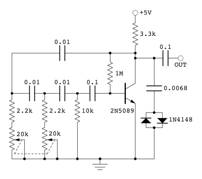
The dual gang 20k pot adjusts the frequency over a range of about 300 Hz to 1000 Hz. The oscillator output is a clean looking sine wave, and amplitude is reasonably constant over most of frequency range. It drops off a bit at the lowest frequency. If there is no need to have the frequency adjustable, the pot can be replaced with fixed value resistors.
The 0.0068µF capacitor and the two diodes form a nonlinear harmonic limiter which is very effective at removing sine wave distortion. It looks like a standard clipper, but there is a difference: The small value of the series capacitance (0.0068 µF) means that it mostly ignores the fundamental, but aggressively clips (attenuates) the harmonics, leaving a clean looking sine wave.
To modulate the output of the DDS module, I used a J310 J-FET operating as a variable attenuator (with attenuation controlled by instantaneous gate voltage). J310’s in the traditional TO-92 package, while still available from major suppliers, are getting expensive. However, they are readily available and inexpensive in the SOT-23 surface mount package. Dealing with these tiny surface mount packages may seem daunting at first, but I’ve managed to accomplish it as can be seen here, and I’m not known for my finesse.
The complete oscillator and modulator circuit is shown below.
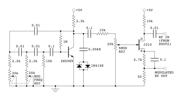
The 10k and 4.7k resistors connected to the J310 drain and source make the circuit appear to be a common source phase splitter amplifier. However, this is not an amplifier; the FET operates as a voltage controlled attenuator. The purpose of the resistors is to bias the FET positive relative to the gate. The gate is biased to ground potential by the DC path through the %Modulation pot. This results in fairly symmetrical modulation of top and bottom of the RF waveform, minimizing the amount of audio signal appearing in the output. This is an advantage that this modulator has over using the Rset modulation method. Modulating the DDS chip using the Rset input only affects the positive peaks of the DDS output signal, leaving the negative peaks unaffected. This results in the audio signal being present in the output when using the Rset modulation method.
The purpose of the 15k resistor connected to the high leg of the %Modulation pot is to limit the maximum modulation level to 100%. The sine wave oscillator puts out plenty of signal, and the 15k resistor limits the output to the correct range. The optimum value for this resistor may vary depending on variations in other component values. So, it’s best to handpick the value to give the correct adjustment range.
Similarly, it’s a good idea to prototype the sine wave oscillator and adjust the 0.01µF capacitors and the 2.2k and 10k resistors to ensure that they give the desired frequency range.
As stated previously, the modulation can be adjusted as high as 100%, but there is a tradeoff. Because of the simplicity of the circuit, the modulation becomes increasingly nonlinear as the modulation percentage is increased. (This is also a problem when using the Rset modulation method.) For modulation levels of 30% or less, modulation nonlinearity is fairly low.
Output impedance of the modulator is 50 ohms making it compatible with other test equipment. Note that the modulator circuit has been optimized to operate from a 5 volt supply. To operate from a different supply voltage, some components will need to be changed.
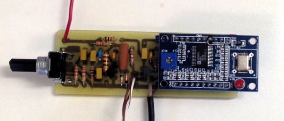
Having got the modulator prototype working well. I designed a circuit board for it, and made provision for mounting the DDS module on it as well. The modulator is shown below with the DDS module installed.
Below is the modulator board without the DDS module, and showing a bit more external wiring.
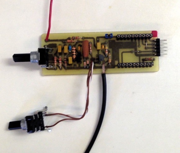
(The above picture shows an earlier revision of the circuit board that does not include the power-on/software reset components.) The 5-pin header on the right edge of the board is the connection to the controller board. Note that the power input for the audio oscillator (red wire) is separate from the DDS module supply. The audio oscillator is intended to operate at 5 volts regardless of the DDS supply voltage. The frequency adjust pot is installed directly on the circuit board, while the % Modulation pot is external. The modulated signal output is via the RG-174 coax at the bottom centre of the circuit board. I realized after fabricating the circuit board, that I could have turned it sideways, and had both pots mounted on the board. However, if I’d continued to make revisions such as this, it probably wouldn’t yet be built.
In order to be compatible with DDS modules that have been modified to bring the RSET line out to the DATA pin, the DATA pin on the modulator board header is connected to a solder pad to allow an external connection. The actual data from the Controller board is connected to pin D7 on the DDS module. This allows the controller to work with a DDS module whether it’s been modified or not.
The signal output (Zout2) from the DDS module passes through a two pin header separating it from the modulator circuit. If direct connection to the modulator is desired, then a shorting jumper (blue jumper plug shown at top centre of the board) can be installed across the pins. Otherwise, the unmodulated DDS signal can be taken off at this point for alternative processing. For example, it may be desirable to pass the DDS signal through a selector switch and then to a separate unmodulated output connector or back to the modulator for output on another connector.
I haven’t implemented a level control feature for the following reasons. A rock steady amplitude level over the entire frequency range was never high on my priority list. I’ve seen a few comments on other sites indicating that the output level of the AD9850/51 is not constant over its entire frequency range, and at the same time noted that their attempts to build ALC circuits have had spotty results. Reading the spec sheet, there’s nothing to suggest that amplitude variation should be a problem. Yet, I’ve observed the output amplitude of the HC-SR08 on my own setup does vary with frequency when not driving a load. I have also noticed that running the RF signal through the modulator circuit has had the effect of minimizing the variations in amplitude. This leads me to believe that this may be an impedance matching issue more than anything else, and that the low impedance load of the modulator may have minimized the problem. If you have a critical need for constant output level, then that is probably a good use for the Rset modification rather than using the post-output modulation circuit that I used here.
I am in the process of building an enclosure for this project, but have nothing to show at this point. I will provide an update to this page once the enclosure is complete.
A zip archive of the printed circuit patterns for the controller board and modulator board along with parts list and component layouts is available for download here:
This concludes the discussion of the physical circuit and its wiring. Information on the PIC controller program and the program files are in Part 2.
Continue to:
Part 2 - Firmware