
Every once in a while, interest gets stirred up in negative resistance devices and various curious circuits start popping up. A negative resistance device exhibits a reverse relationship between voltage and current. In a normal electronic device, the current through the device increases as the voltage across its terminals increases. In some cases, as with resistors, this relationship is linear, and the device obeys Ohm's Law:
|
where R is the constant of proportionality we know as Resistance.
In other devices, the relationship is non-linear. An example is a semiconductor diode, that obeys the Shockley diode equation:
 |
In both of these examples, whether linear or not, the current always increases monotonically as voltage increases.
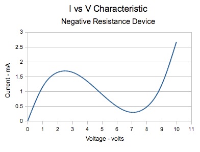
In a negative resistance device (for example, a tunnel diode), current and voltage both start at zero, and current will increase with increasing voltage up to a certain point, after which the current begins to decrease with further voltage increases. This region, where the current decreases with increasing voltage is known as a negative resistance region, or more precisely, a negative incremental resistance region. The following graph shows the relationship between current and voltage for a negative resistance device. The negative resistance region ranges from approximately 3 volts to 7 volts.
For this discussion, I'll abbreviate negative resistance device to NRD.
The type of NRD described above, is known as a voltage controlled NRD or N type (because the I-V curve is N shaped as shown in the above graph). There is also a current controlled NRD, or S type (due to an S shaped I-V curve). Another type referred to as the Z type is essentially a minor variation of the S type. I will limit the present discussion to the N type NRD, and deal with the S (and Z) type NRD later.
Many articles have been devoted to LC oscillator circuits using NRDs, but very few devoted to NRD amplifiers. The usual explanation for how a negative resistance LC oscillator works is that the negative resistance compensates for (cancelling out) the positive resistive losses in the LC tank. That's a perfectly valid explanation, but may not be the easiest thing to visualize in terms of what is happening in the circuit in realtime. The question then is:
Is negative resistance just some arcane effect that somehow keeps LC oscillators oscillating, or does the device have actual gain in the same sense as a more traditional device such as a transistor?
It's reasonable to assume that in order for a circuit to oscillate, there must be some sort of gain to keep the oscillations from dying out. However, relaxation oscillators work on the principle of a capacitor charging up until a certain trigger voltage is reached, and then some type of active device 'fires', discharging the capacitor. The cycle then repeats. In this case, it's hard to reconcile the concept of gain with a device which fires on and off. (To muddy the waters even more, S type NRDs often appear in relaxation oscillator circuits.)
So, this needs further study. Load line analysis will help answer that question. I must give this warning though. The discussion that follows is mainly theoretical (though not overly complicated), and ignores certain realities. However, some real circuits will be tested to see how they compare to theory.
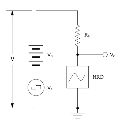
Consider the following circuit, which includes a power supply VS, an output load RL, and a negative resistance device NRD which has the I-V characteristic as given in the previous graph. The output voltage VO is taken between the upper terminal of the NRD and ground.
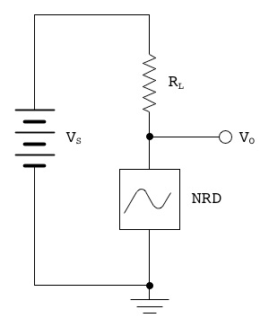
How do we determine the output voltage?
Obviously it depends on the values of the supply voltage, the load resistance, and the I-V characteristic of the NRD. The voltage drop across RL is equal to the current through it multiplied by its resistance. The voltage VO must then be:
 |
(1) |
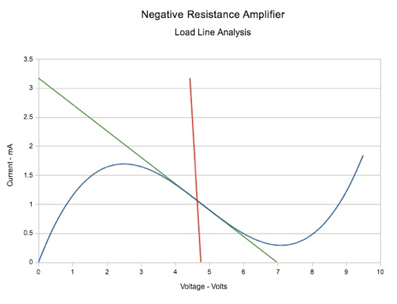
In this example, let's say that VS is 6 volts, and RL is 1 kΩ.
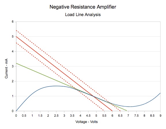
We can plot VS–I×RL versus I on the same graph as the NRD's I-V curve. This is called a load line. We get the following result:
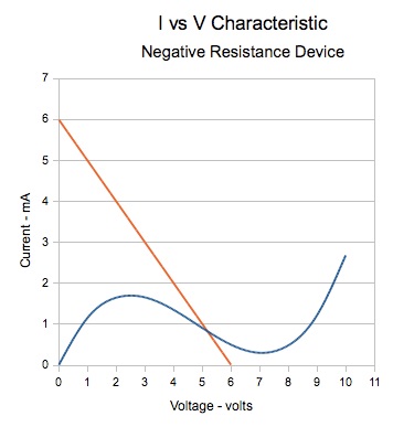
Since the load RL is a linear resistance, the load line is a straight line. It crosses the horizontal axis at V=VS and crosses the vertical axis at I=VS/RL. This gives us a very quick way to draw a load line. We need to know only those two points, and then draw a straight line between them to get the load characteristic. Now here is the important part:
The point where the load line crosses the NRD characteristic curve, is where both of the circuit constraints are met, and so this is the quiescent point where the circuit operates.
In this case, VO=5.2 volts, and I=0.8 mA.
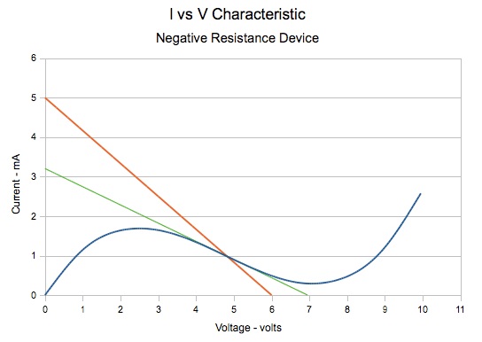
Now, if we draw a line, tangent to the NRD I-V curve at this crossing point, we get the following green line with a slope of about –0.46 mA/Volt, which is its incremental conductance. The reciprocal of conductance is resistance. Hence the incremental resistance is 1/(–0.46) = –2.2 kΩ (note the minus sign). This incremental (negative) resistance value will be represented by the variable RN, and by convention (chosen here), its value will be negative.

It can be seen that the tangent line is a reasonable approximation to the curve over the range of about 3.75 to 6 volts. It intersects the vertical axis at I=3.2 mA. This y-intercept current value will be represented by the variable I0.
From these numbers we can come up with an equation for the current/voltage relationship of the NRD:
 |
(2) |
or in this example case:
 |
where V is volts and I is mA, when RN is in kΩ.
Of course this is only valid over the range 3.75 to 6 volts, the middle of the negative resistance region.
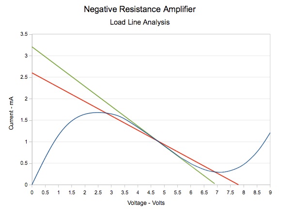
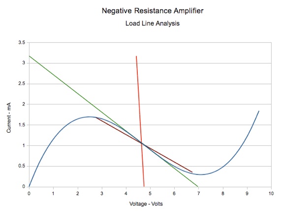
At this point, we will adjust the value of the load resistor RL from 1 kΩ to 1.2 kΩ. This will move the quiescent point closer to the centre of the linear region:
We now have a quiescent point of V=4.8 volts and I=1 mA.
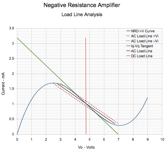
Now that we have most of the preamble out of the way, it's time to add an input signal, and see what happens. To keep things simple, the input signal will be an ideal voltage source VI that produces a square wave switching between –0.5 and +0.5 volts. The revised schematic is shown below:
The net voltage V applied across RL and NRD is equal to VS+VI, giving a range of 5.5 to 6.5 volts. This causes the RL load line to shift left or right by ±0.5 volts as indicated by the dashed load lines in the following graph:
Note that the load line slope does not change, because its slope is dependent only on the load resistance value, which is constant. The points where the shifted load lines intersect with the NRD I-V curve will correspond to the minimum and maximum values of the instantaneous output voltage VO. These values are approximately 3.7 and 5.9 volts. So, when the input voltage VI varies by 1 volt, the output voltage VO varies by 5.9 – 3.7 = 2.2 volts. Thus, we have a voltage gain of 2.2.
That's all well and good, but we can also apply an AC voltage to the primary side of a step up transformer and get a voltage gain on the secondary side. So, have we really accomplished anything? A transformer may give a voltage gain, but there will be no power gain. In fact, a transformer will give a small power loss due to its internal losses. So, let's have a look at what happens to power with the NRD circuit.
With no input, the current is 1 mA and the power dissipated in the load resistor is:
 |
In the first half cycle, when the input voltage is –0.5 volts, the net circuit voltage is6 – 0.5=5.5 volts, and the current in the circuit is 1.5 mA. The power delivered to the load is:
 |
In the second half cycle, when the input voltage is +0.5 volts, the net voltage is 6+0.5=6.5 volts, and the current in the circuit is approximately 0.5 mA. The power delivered to the load is:
 |
Therefore, with the input signal applied, the average power delivered to RL is the average of the minimum and maximum instantaneous power values or:
 |
Meanwhile, the instantaneous power delivered by the input device is equal to its instantaneous voltage multiplied by the instantaneous current flowing in the circuit. For the –0.5 volt half cycle, the current is 1.5 mA, giving an instantaneous power input of –0.75 mW. For +0.5 volt half cycle, the current is 0.5 mA, giving an instantaneous power input of +0.25 mW. The average power input is the average of the power delivered in the two half cycles or:
 |
A negative value. That is, the signal source is not putting power into the amplifier; it is receiving power from the amplifier!
Strictly speaking, it is receiving power from the main power supply VS, due to the behaviour of the NRD. That can be good or bad depending on what we are trying to accomplish. In the case of an LC oscillator, we could replace the input signal generator with an LC tank. Any voltage generated by the tank circuit will cause in-phase energy to be fed back from the rest of the circuit, thereby maintaining oscillation. That's fine for oscillators, but we were trying to make an amplifier. Let's suppose our input device is a dynamic microphone, and we want amplification, not oscillation. Feeding power back into a dynamic microphone will make it behave like speaker, which is probably not a good thing.
We will now briefly digress from the graphical analysis to look at some numbers. The reason for drawing the tangent line on the NRD I-V curve, and then developing an equation for it, is that we can solve the linear equation quite easily and get another view of what is going on.
If we combine equations (1) and (2) from above, we get an expression for VO in terms of V, where V=VS+VI
 |
Multiplying out the terms:
 |
Combining terms of VO, we get:
 |
Then:
 |
And:
 |
Notice that the second term on the right side of the equation is a constant and simply contributes an offset, or bias voltage. Incremental variations of VO are therefore due solely to the first term. Thus, it's apparent that the voltage gain of the circuit is equal to the constant part of the first term 1/(1+RL/RN). Hence:
 |
(3) |
which can be simplified further to:
 |
(3a) |
where AV is the voltage gain. It should be pointed out that formula (3a) is exactly the same as the attenuation ratio in a voltage divider, which makes perfect sense, because the circuit being studied here, is in fact a voltage divider, where the lower resistor has a negative value.
This formula tells us several things:
Voltage gain is negative when |RL/RN| > 1;
Voltage gain is positive when |RL/RN| < 1;
Voltage gain approaches ±infinity as |RL/RN| approaches 1.
This also resolves a possible misconception: "that the net incremental resistance around the circuit must be negative in order to cancel out all losses and provide net gain." It can now be seen that this is not true. The net resistance can be positive and still have gain.
The formula for voltage gain leads directly to a formula for power gain which is:
 |
(4) |
Or:
 |
(4a) |
where AP is power gain, and AV is voltage gain.
The absolute value of the voltage gain will never be less than or equal to one. Therefore, when voltage gain is positive, the power gain is negative, and when voltage gain is negative, the power gain is positive.
Now back to our amplifier circuit: if we don't want to feed power back into the input device, then we need to make the voltage gain negative, and we do that by making the magnitude of the load resistance RL larger than the magnitude of RN. In the example circuit, it means that we need to make RL>2.2 kΩ.
Let's make RL=3 kΩ and see what happens. Adjusting the supply voltage to 7.8 volts brings the quiescent point back to the middle of the negative resistance region, as shown in the next graph:
Unfortunately, we have a problem. The load line crosses the I-V curve in three places: at 2.75, 4.75, and 7 volts. Any of these is a valid and stable operating point. However the intention was to have the quiescent point at the 4.75 volt crossing point. This immediately shows an advantage of the graphical method. The problem is obvious at first glance. If we had simply adopted the formula using the linear approximation, the problem might not be discovered until the circuit was built.
This circuit could be forced to the desired quiescent point by controlling the way that the circuit is powered up, but a sudden transient could cause the quiescent point to jump to one of the other possible states, locking up the circuit. So, this would not be a good design in any event.
Let's make a small revision to the circuit as follows:
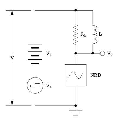
An inductor has been added in parallel with the load resistor. If the DC resistance of the inductor is very small compared to RL then the 'static' load line changes to a nearly vertical line. We now reduce the supply voltage to 4.75 volts so that the load line again passes through the middle of the negative resistance region:
Because RL has been bypassed by a resistance of nearly zero, the DC voltage gain is now approximately unity. The inductance value L is chosen so that at the frequencies of the signals we wish to amplify, the inductive reactance will be much larger than the resistance of RL. So, as frequency increases, the inductive reactance increases, and the load line pivots at the quiescent point, rotating until at operating frequencies, the slope of the load line is once again the same as it was before RL was bypassed, shown here in dark red:
The next graph shows the AC load line shift due to the input signal. In this case, because the voltage gain is much higher than before, the input signal has been reduced to ±0.25 volts. With this small input swing, the full region of negative resistance is traversed.
From this last graph, it appears that we have succeeded in designing an amplifier using a negative resistance device. However, we need to be careful. If the load line slope is very close to the slope of the NRD I-V characteristic, as it is in this case, and if we expect to get a large output swing, there is still a possibility of multiple intersections between the load line and the I-V curve, which can cause distortion of the signal. There is also some concern about the use of reactive components (i.e., the inductor), which are likely to cause instability at some frequencies.

At this point, I decided to construct a test circuit to attempt to confirm the predicted behaviour. I constructed Ramon Vargas Patron's variation of a lambda diode, in my case using a J310 in place of the MPF102 FET. The circuit for the lambda diode is shown at the right.
I measured the lambda diode I-V characteristic, which is graphed below.
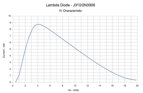
As can be seen, it has a very nice broad and fairly linear negative resistance region from 4 to 18 volts.
Experimentation is still in progress, but initial tests verify that when the load resistance RL is less than −RN then the circuit does feed power back to the source, and if that source is an LC tank, then it will oscillate. This merely confirms what is already well known.
What is of more interest to me, is what happens when RL is slightly greater than −RN. In this case the foregoing analysis predicts that the circuit should behave as an inverting amplifier. Not surprisingly, the use of an inductor in setting the bias, did cause some circuit instability. However, at certain bias settings, the circuit was stable, and I was able to measure a small power gain of about 2. At bias settings and RL values which should have provided significantly more power gain, the circuit became unstable and started to oscillate.
If one wishes to pursue a more practical negative resistance amplifier, then further work needs to be done in the development of a stable bias circuit.
The purpose of this study was to determine whether amplification without oscillation is possible, theoretically and in practice, and that has been demonstrated. However, except for the novelty value, there is very little reason to encourage the use of negative resistance devices. They suffer the disadvantage that the input signal cannot easily be isolated from the output signal. Therefore, there must be some compelling advantage of a specific negative resistance device that makes it worth the trouble in a given application. To date, they have generally been limited to use at microwave frequencies.
At some point in the future, as time permits, I hope to do a similar analysis of S-type negative resistance devices.
With regards to load line analysis, this is one of many graphical design techniques that have been taught in engineering classes over the years. I was told not too long ago that students are no longer taught load line analysis. I don't know if this is true or not. If it is, then I think it's a terrible shame. We can use computers and numerical methods nowadays to solve nearly any problem, but a picture is still very valuable in making things easily understandable.
Back to:
Radio/Electronics Theory
Home
This page last updated: March 31, 2023
Copyright 2012, 2023 Robert Weaver