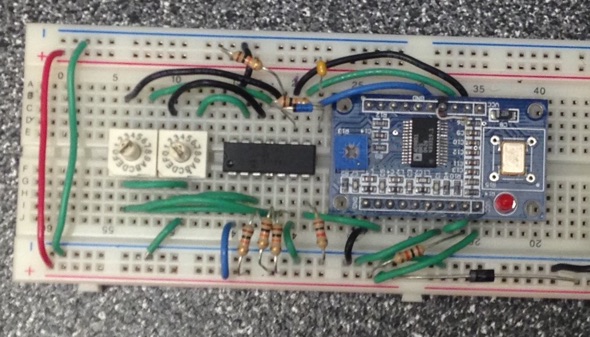
No sooner had I uploaded my General purpose DDS controller project to this site, than I became interested in a conversation on a radio related forum, where it was suggested that it might be useful to have a minimal parts count frequency generator to cover the medium wave broadcast band. I suggested that the LCD display could be eliminated, and frequency adjustment could be by means of a pair of hex coded DIP switches. One switch would set hundreds of kilohertz, and the other switch would set tens of kilohertz. This would give enough adjustment range to more than cover the North American MW band with 10 kHz channel spacing. I quickly breadboarded the circuit, and adapted program code from my general purpose DDS controller.
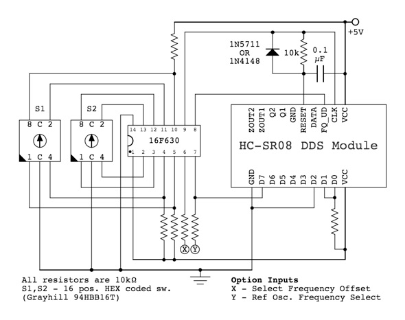
Here is the circuit diagram:

As with the previous DDS controller project, a 16F630 is used for the microcontroller. This is an older processor, which can be programmed by the inexpensive PICkit2 or its clones (or newer PICkit versions). Note that on the DDS module, both Vcc lines are connected together, and so power feeds through to supply the PIC controller. Also, note that on the DDS module, D7 and DATA are the same signal. So pin 7 from the PIC can be connected to either one.
If the DDS module is one of the ones supplied with a 3.3 volt oscillator, then the entire circuit will run just fine at this lower voltage. The PIC is designed to operate at this lower voltage as well as at 5 volts.
The line coding of the hex DIP switches is indicated on the diagram: 1,2,4,8 and C for common. Other brands/models of switches may have a different pinout. Also note that other models or brands may have two or more C (common) terminals which must be connected together in order for the switch to work correctly. This is because one of the commons may only connect internally to the 1 & 2 outputs while the other common connects internally to the 4 & 8 outputs or some other similar partial connection. It's best to check for continuity between the common pins to be sure. If there's no continuity, then connect the commons externally.
After experimenting with these DDS modules for some time, I’ve noticed that on rare occasions, the DDS module fails to start up properly, and it’s necessary to cycle the power to get it going. I suspect that the source of this problem is related to the DDS chip’s power on reset sequence. On my earlier project, I had initially connected one of the PIC outputs to the DDS reset line so that the PIC program would force a reset upon startup. I later deleted this in order to free up a needed I/O line, noting that most other DDS controller projects that I’d seen simply kept the reset line permanently grounded. For the current project, I decided to implement a reset function for better reliability. Since there was no spare PIC I/O line, I added the simple timing network consisting of the diode, capacitor and resistor connected between the clock line and the reset line. When power is applied to the circuit, the PIC I/O lines are in high impedance state and with one side of the capacitor connected to +Vcc, the reset line is immediately pulled high, holding the DDS in reset. Once the PIC has initialized, it pulls the clock line low, and the capacitor discharges through the diode, pulling the reset line low. This causes the DDS to start normal operation. When the PIC sends data to the DDS, the positive clock pulses are too narrow to affect the reset line due to the long RC time constant. However, the PIC can reset the DDS whenever necessary, simply by raising the clock line to logic 1, and holding it there for a few milliseconds. If one wishes to keep the circuit extremely simple, then the resistor, capacitor and diode can be eliminated, and the reset line permanently connected to ground. However, the DDS may not always start up reliably.
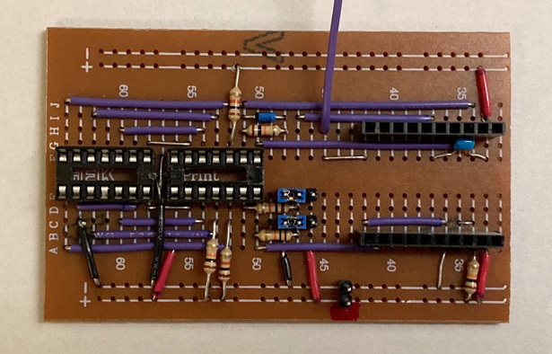
The circuit was arranged to make wiring as simple as possible. There’s no need to make a printed circuit board; the circuit can be quickly built on perfboard or Veroboard (aka stripboard), as shown below:

As can be seen, the conductor arrangement matches that of the white plastic proto board shown in the photo at the top of the page. This makes it easy to transfer the design from the prototype to the final circuit board.
The following photo shows the board with the sockets, passive components and jumpers installed.

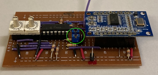
The completed board with the DDS module plugged in is shown below.

Note, the area annotated with the green circle shows plug jumpers for setting the state of inputs X and Y. With the jumper in the lefthand position, the input is logic 0. With the jumper in the righthand position the input is logic 1. Further details of these inputs are given below in the Controller Program section. Both X and Y inputs are shown on Veroboard trace 47 but they are not connected together, because the trace has been cut between point C and point D. (Refer to the Point letters and trace numbers silkscreened on the board.) No other traces have been cut. However, there are 3 places on the foil side of the board where adjacent traces have been bridged in order to make connections where there was not enough room for jumpers on the component side. These are:
For this project, I took the opportunity to simplify some of the code used in the general purpose DDS controller. The keyboard read routine was replaced with a routine to read the rotary switches, and all of the frequency sweeping code was deleted. Also, I got rid of the lookup tables used for frequency calculation. Since the table values were all simple multiples of the same base value, it made sense simply to store that single value and calculate the ten coefficients when needed. Multiplication by 2 though 9 is done by repeated additions which is fast enough for this application. Eliminating the lookup tables saves considerable program memory. This allows storing the FTW (frequency tuning word) base values for both 125 MHz and 180 MHz reference oscillator frequencies. When the circuit is powered up, the PIC checks the state of input Y and selects the correct base value accordingly. For 125 MHz operation, input Y should be connected to +Vcc (logic 1), and for 180 MHz, it should be grounded (logic 0).
A second option selection input is provided: input X which causes an additional frequency offset to be added to the DDS frequency setting. As currently programmed, the offset is 1600 kHz. Unlike option input Y which is only checked at startup, this input is monitored continuously. When this input is connected to ground (logic 0), the offset is disabled. When connected to +Vcc (logic 1), the offset is enabled. Since the rotary switches can select any frequency from 0 to 1590 kHz in 10 kHz steps, this offset feature doubles the frequency range, giving continuous coverage from 0 to 3190 kHz in 10 kHz steps. The offset value is stored in EERAM memory, and I may add a method in the future to allow the user to change the value. For example, it might be handy to have the offset value set to the receive IF frequency for a transceiver application. For now, the value can only be changed in the source code file, and the project recompiled.
A zip archive of the source code and hex file for the program is available for download here:
Note: There was a bug in an earlier version of the firmware that prevented it from working correctly with AD9850 DDS chips. It worked correctly with AD9851's. This current version works correctly with both AD9850 and AD9851. If you are unable to get an AD9850 up and running, you may have an older version of the firmware. Please download this current zip file.