Switch-mode B+ Supply
Occasionally, there is need for a high voltage supply for various electronics
projects. A couple of my projects which fall into this category are:
- Three
Tube Superhet Receiver
- Nixie
Display
As with any high voltage circuit, a word of caution is in order. These
circuits can generate high voltages at sufficient current levels to
be deadly. Proceed accordingly, and at your own risk.
A small switch-mode supply, such as presented here, is not capable of
delivering as much current as a power supply operated directly from
the power mains. However, it can still deliver a serious or even
deadly shock. Don’t be misled by its small size!
Here is the schematic for the circuit I developed:
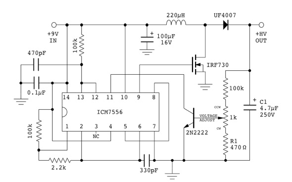
It is a standard boost converter circuit.
Parts
Parts values are as indicated. The ICM7555 is a CMOS version of a dual 555
timer. This was chosen over switch-mode regulator ICs, because it’s
readily available in a standard DIP package, making it easy to mount
on the circuit board.
The IRF730
is a high voltage MOSFET. Other types with similar voltage ratings
may be substituted, as long as the turn-on gate voltage is suitably
low (5 volt TTL level, or less), and the breakdown voltage is
suitably high. The IRF730 was the most inexpensive one that I could
find at the time of construction.
The UF4007
diode should not be confused with a 1N4007 diode. These parts are not
interchangeable. The UF4007 is an ultrafast rectifier which is
required in a high frequency switching power supply.
The
inductor may be either a Coiltronics DR127-221-R, or an AlfaMag
SWF-1.4-220. Other types will be suitable as well, but the circuit
has been tested with these two inductors and they work well, giving
good efficiency.
Operation
Output voltage is adjustable from below 50 volts to over 400 volts. However,
if operation above 200 volts is required, then the voltage rating of
C1 must be increased accordingly. The supply can deliver over 25 mA
at 90 volts. This was the primary design requirement, because one
application is as a power supply for a vintage Zenith Transoceanic
receiver which has this power requirement. At this output load, the
overall circuit efficiency is 82%.
I have not
yet done any exhaustive testing of the power supply to find its
maximum voltage/current limitations. In testing so far, neither the
MOSFET nor the inductor has shown any detectable temperature
increase. The MOSFET is supplied in a TO-220 package suitable for
heatsink mounting, but a heatsink is not required in this circuit.
Circuit Notes
The operation of a boost converter circuit is fairly straightforward. A
detailed explanation is given on Wikipedia.
However, I will provide a more brief explanation here.
The timer turns on the MOSFET, allowing current to flow from the power input,
through the 220µH inductor, and through the MOSFET to ground.
Because of the inductance, current flow cannot change instantly, and
so it starts at zero and then increases steadily. If the MOSFET were
to remain on indefinitely, the current would reach a level
sufficiently high to burn something out. However, the MOSFET is
switched off before that happens. Because the current through the
inductor cannot stop instantly, the only path is through diode and
the electrolytic capacitor C1. The voltage at the inductor will
increase to whatever value is necessary in order to maintain the
current flow. This is the principle that causes the voltage across
the capacitor to exceed the circuit input voltage. The output voltage
is regulated by a feedback circuit consisting of the resistor voltage
divider network across C1, and the NPN transistor. This controls the
charging current, and hence the time constant, in one of the timer
sections, resulting in a variable pulse width signal to control
MOSFET on-time. The second timer in the ICM7555 runs at a constant
frequency to control the MOSFET switching frequency. The result is a
constant frequency pulse width modulation (PWM) signal that maintains
the output voltage over a wide range of output load conditions and
varying input voltages.
This circuit operates at approximately 24 kHz. This is quite low for
switch-mode power supplies which typically operate at hundreds of
kHz. However, this frequency was chosen because it is high enough to
be above audio range, high enough to use reasonably small value
inductors, but at the same time low enough that it won’t generate
massive amounts of RFI (Radio Frequency Interference). The low noise
requirement is important for radio applications. Even at a switching
frequency of 24 kHz, this supply still produces significant harmonics
right up to shortwave frequencies. Therefore, RFI mitigation, in the
form of shielding and filtering is still required.
Construction
This circuit is quite forgiving of construction methods, but best performance is
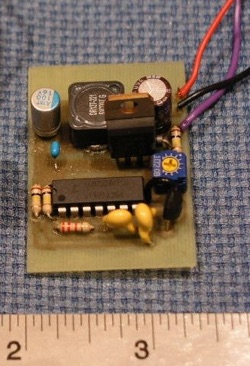 obtained when built on a printed circuit board, following good high
frequency design practices. The prototype is shown in the photo to
the right. Circuit board dimensions are 1.75” x 1.375” (45mm x
35mm). The 220 µH inductor is the small square black part near the
top of the board partially hidden by the MOSFET. It is a Coiltronics
DR127-221-R. This is a shielded ferrite core inductor which minimizes
radiated RFI. The inductor is intended for surface mounting, and may
be installed on the foil side of the board if desired. However, I
simply soldered a couple of short bare leads through the board, and
then soldered the inductor onto these on the component side. The
circuit board foil pattern and component mounting information are
available in this
zip file. The foil pattern is mirror image, suitable for use with
the toner transfer method, of printed circuit construction. The
circuit board includes no output filtering to remove RFI, and
therefore an external filter may be required depending on the
application. RFI is discussed in the following section.
obtained when built on a printed circuit board, following good high
frequency design practices. The prototype is shown in the photo to
the right. Circuit board dimensions are 1.75” x 1.375” (45mm x
35mm). The 220 µH inductor is the small square black part near the
top of the board partially hidden by the MOSFET. It is a Coiltronics
DR127-221-R. This is a shielded ferrite core inductor which minimizes
radiated RFI. The inductor is intended for surface mounting, and may
be installed on the foil side of the board if desired. However, I
simply soldered a couple of short bare leads through the board, and
then soldered the inductor onto these on the component side. The
circuit board foil pattern and component mounting information are
available in this
zip file. The foil pattern is mirror image, suitable for use with
the toner transfer method, of printed circuit construction. The
circuit board includes no output filtering to remove RFI, and
therefore an external filter may be required depending on the
application. RFI is discussed in the following section.
RFI Mitigation
The MOSFET switches extremely quickly,
which results in high operating efficiency. When fully off, the
MOSFET consumes no power. When fully on, the power dissipated in the
MOSFET is i2RDSon. The value of RDSon is extremely low in these types
of MOSFETs, resulting in very low power losses when on. However,
significant power dissipation can occur if the device switches
slowly. During the switching period, both the voltage and current are
significant, and lead to significant power dissipation and heating of
the device. For this reason, the devices are designed for the fastest
possible switching speed. Unfortunately, the extreme switching speed
causes switching transients with extremely fast rise times, resulting
in the generation of significant amounts of RFI.
To eliminate or minimize RFI, the first step is to install the power
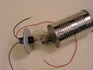 supply in a shielded enclosure. This prevents direct radiation of
RFI. For initial testing, I mounted the power supply circuit board
inside a small tin can. The power leads pass through a ferrite sleeve
to reduce conducted RFI. With just this level of RFI abatement, I
decided to test it on my Three
Tube Superhet. On the medium wave band, performance was better
than expected. However, there were several frequencies across the
band where the amount of generated interference was unacceptable. I
then tested it on the shortwave band from 5000 to 6000 kHz.
Surprisingly, the RFI was far worse at these higher frequencies, and
most of the received radio signals on this band were obliterated. The
reason became apparent when I connected an oscilloscope to the power
supply output while under load. There was noticeable ringing on the
waveform whenever the MOSFET switched. The ringing frequency appeared
to be at approximately 5000 kHz, right in the band where the radio
was operating.
supply in a shielded enclosure. This prevents direct radiation of
RFI. For initial testing, I mounted the power supply circuit board
inside a small tin can. The power leads pass through a ferrite sleeve
to reduce conducted RFI. With just this level of RFI abatement, I
decided to test it on my Three
Tube Superhet. On the medium wave band, performance was better
than expected. However, there were several frequencies across the
band where the amount of generated interference was unacceptable. I
then tested it on the shortwave band from 5000 to 6000 kHz.
Surprisingly, the RFI was far worse at these higher frequencies, and
most of the received radio signals on this band were obliterated. The
reason became apparent when I connected an oscilloscope to the power
supply output while under load. There was noticeable ringing on the
waveform whenever the MOSFET switched. The ringing frequency appeared
to be at approximately 5000 kHz, right in the band where the radio
was operating.
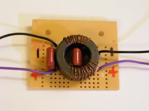
The
next step was to build a low pass output filter to remove this high
frequency noise. After trying of couple of different filter
configurations, I obtained the best results with a differential mode
choke consisting of a 25 mm diameter by 12 mm long ferrite toroid,
with two 9 turn windings of #24 AWG magnet wire. The ferrite is of
the type designed for RFI filtering, and has a relative permeability,
µR,
of about 6500. This results in an inductance of about 640 µH per
winding. Shunt capacitors (0.047 µF) were placed across both input
and output sides of the choke.
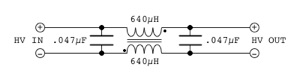
This resulted in the elimination of the high frequency ringing, and
reduced the sharp switching transient to little more than a very low
level ripple.
It should be noted that both the positive and negative high voltage leads pass
through the filter and therefore the negative lead is not common to
the negative input of the low voltage power input. My primary concern
at this stage was to determine whether the HV output could be made
sufficiently noise free to operate a radio receiver. So, I had no
immediate concerns about the isolation of the negative leads. The
power supply was powered from a six volt lantern battery which had
its negative side isolated from the HV negative lead. Given the
encouraging results of these tests, the next step is to design a more
advanced filter that will allow for a common ground point for both
the high and low voltage negative leads.
Since one of the applications of this converter circuit was the B+ supply of a
battery operated radio, it would be convenient to have it switch on
and off automatically according to whether the tube filaments are
drawing power. To that end I designed a current
switch circuit that can be found at the link below.
Continue to:
Current Switch Circuit
Back to:
Projects
Home
This page last updated: March 27, 2023
Copyright 2014, 2023, Robert Weaver